The 2nd version PCB's arrived last week, and I jumped in and assembled them and I think they came out looking really nice:
Controller Front:
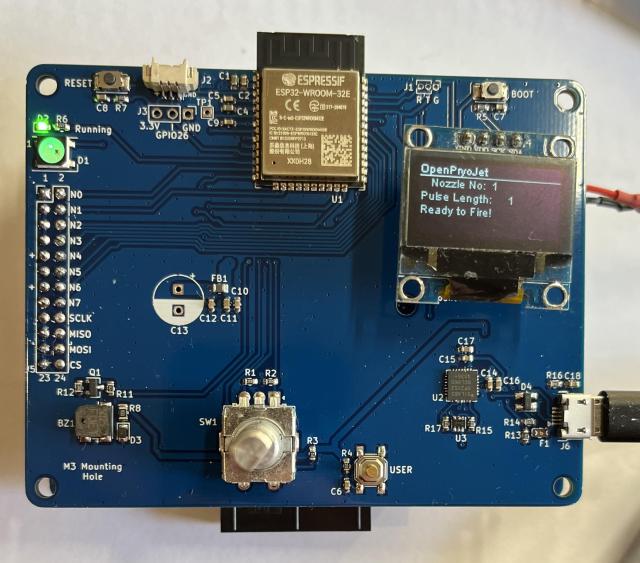
- OPJ-Controller_V0.6_sml.jpg (58.25 KiB) Viewed 34826 times
Driver Front:
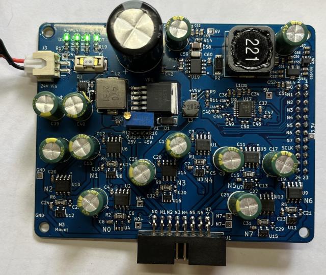
- OPJ-Driver_V0.6_sml.jpg (75.52 KiB) Viewed 34826 times
So the changes between the V0.5 and V0.6 PCB versions are mainly that it now has individual ADC monitoring of each nozzle current, and a cleaner ADC voltage reference and 3.3V lines. The only mistake was that I used a 0805 footprint for a 12V zener diode and instead I purchased a SOD-123 sized zener. This is easily fixed with a short 6mm bit of bodge wire.
It took a day or so before I could get my code to read the ADC128S102 ADC SPI based IC. I had never written SPI code before and was a bit daunted by it, but in the end it turned out to be very easy, and I am getting around 25u Second read time for a 12bit value.
Here are some labelled plots (via SerialPlot), of various firings:
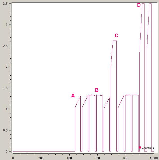
- ADC_Plots.jpg (26.42 KiB) Viewed 34826 times
A: is two firings of a ~39 ohm filament. You can see the current rises over time.
B: two firings of a 22 ohm resistor
C: a filament being fired but ADC cuttings out/limiting (0.04 ohm sense resistor) the readings.
D: I then moved to using a Nozzle with a smaller 0.03 ohm sense resistor and got these two plots. They are being limited due to reaching the motor driver current limit.
So, all is good, but then late one night, I had a go at trying to monitor the motor driver voltage and produced this horrid graph:
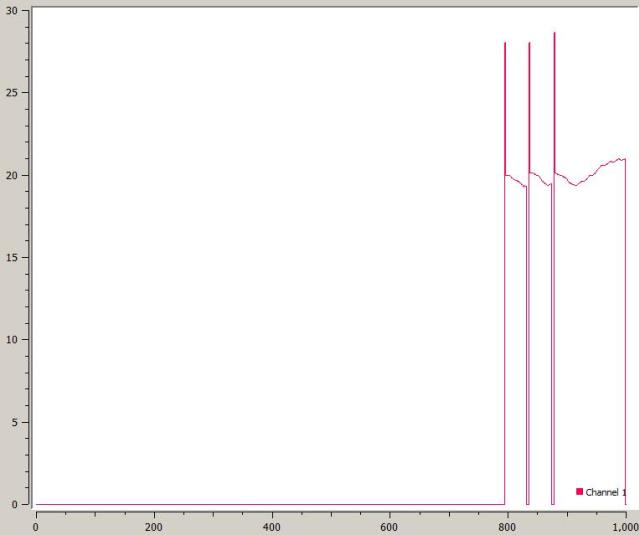
- Bad_ADC.jpg (14.37 KiB) Viewed 34826 times
To me, it looked like there was a huge voltage sag when the Nozzle was filing, going from near 30V down to 19V! I didn't sleep well that night. Later the next day though, I re-checked the circuit and it all looked ok. I put together a voltage divider and checked my bench power supply to make sure it was supplying the correct current, and it could put out a max. of 26V at 4A, so that sounded ok. Late that evening, I delved into the code and sure enough, found the large pulse was a buffer over run which was quickly fixed (what was I thinking, why did write the code that way?). The last code error that was giving me the 19V readings was me not doing the maths correctly. Once I fixed that, I was getting a solid 30 odd volts.
This last graph is a total of 6000u seconds, with the hand drawn green trigger pulse showing approximately when the nozzle is firing for 1000u seconds. It kind of looks ok. Previously oscilloscope readings show that there is a bit of a sag, but maybe only 1V or so, which sounds ok to me. More on this in a later post.
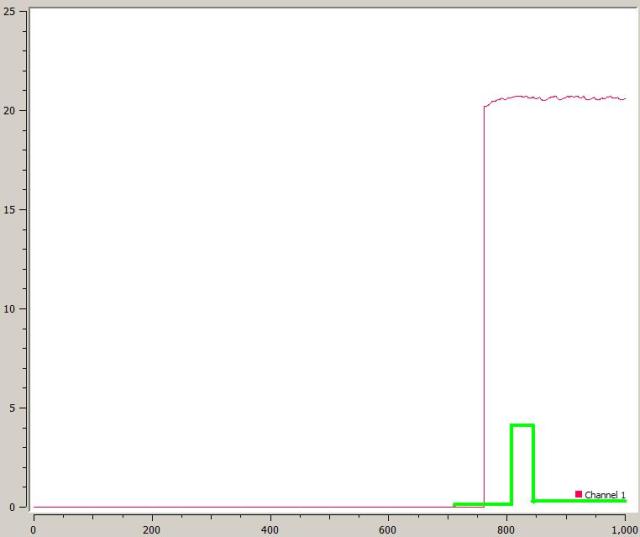
- Good_ADC.jpg (12.34 KiB) Viewed 34826 times
I have already drawn up a new schematic and laid out the PCB with the following small changes:
* fixed the Zener footprint
* added a power switch, which switches a MOSFET on/off. Handy when doing Dev work
* added a 5V reference IC to give a more precession voltage for the ADC
* added an extra resistor to the 6V DC-DC feed back divider, so the output voltage can be better tuned
* the next version V0.7 will be done in hot Red solder mask
