As I mentioned above, I have found three different Ideal Diode circuit diagrams on line (note the resistor values in #1 and #2), these are:
1)

- ideal-diode-schematic.jpg (53.85 KiB) Viewed 6767 times
2)

- ideal-diode-schematic2.jpg (85.81 KiB) Viewed 6767 times
3)

- ideal-diode-schematic.3.jpg (12.46 KiB) Viewed 6767 times
These are all based on a transistor current mirror arrangement. I have previously unsuccessfully tested circuits 1 and 2. Maybe the problem was the MOSFET, or dual transistor package I was using and that was why it failed. Failed, in that I would always see a residual 2.6V at the input with a voltage present at the output. But this was meant to be a Ideal Diode, so I shouldn't be seeing no where near that high a voltage being passed through to the input. This is the reason I created the Ideal Diode test PCB:

- ideal-diodeV1.0_sml.jpg (315.46 KiB) Viewed 6767 times
Note: in the above photo, I am feeding 12V in INPUT 2 through circuit 5 and then backwards through circuit #3. You can see the bright(er) LED in #5 and a very faint LED in #3.
I have marked each of the circuits with a texter. 1 & 3 are based on circuit 3 above (triple resistor), and have a AO3401 and RU30L30 MOSFET. Both of these never turned the MOSFET on as much as the other design.
PCB circuits marked 2, 4 and 5 are based on my schematic shown below (and circuits 1 & 2 shown above). I spent a lot of time experimenting with these.
I have laid out all three examples and placed some with variable resistors, so I can tinker with the values to see what happens. Here is main circuit:
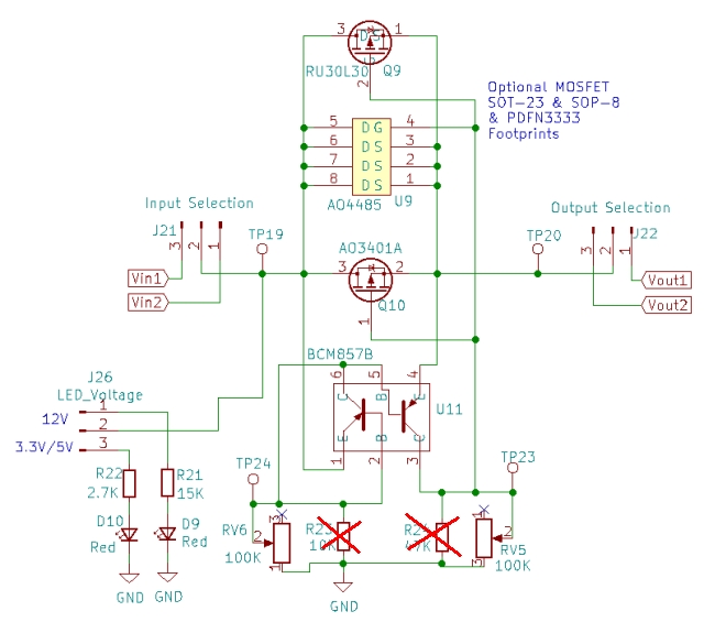
- ideal-diode_schematic.jpg (112.53 KiB) Viewed 6767 times
This is similar to diagrams 1 and 2 above. I have included pads for three different MOSFET footprints, so I can hot air different ones in and out of the PCB. Same with the fixed and variable resistors for the transistors. Each circuit can be isolated for the others using the colourful jumpers.
It's been a while since I designed up the PCB and I quickly reminded myself to review the MT9700 high side switch IC datasheet - AFTER I had let out the magic smoke by putting 12V into the 3-5V IC

Luckily I have a stash of them, so it was easy to hot air another one back into place.
So after 7 or so hours of playing around with the PCB, what have I found out? They all *kind* of work when inputting 12V, I say kind of, because I think ALL of them where mostly operating with a partially biased MOSFET and perhaps the body diode was helping to pass the current through to the output.
What worked best was diagram #1, with the 10K and 47K resistors transposed, ie: the 47K ohm resistor on the left side of the diagram. 90K and 20K values work as well, and the MOSFET gate was driven a bit stronger.
Ok, some data. I tested two MOSFETS: AO3401 (footprint=SOT23, 30V 4A, Vgs=12Vmax) and a RU30L30 (footprint=PDFN3333, 30V 30A, Vgs=20Vmax) both P-channel. Yes, the AO3401 Vgs was pushed to the max and survived, but not recommended. I tested both the DMMT5401 and BCM857B dual matched transistors, with no difference found between the two dual transistors packages.
A) Using my diagram, with RV6 set to 10K and RV5 set to 47K ohms, the MOSFET gate was at 8.9V with respect to GND, or -3.1V from the input voltage. I measured 49mV drop across the MOSFET with a load of 510mA at 12V input. This is a 24.99mW power loss across the MOSFET.
B) With RV6 set to 47K and RV5 set to 10K ohms, the MOSFET gate is driven harder at 1.93V with respect to GND or -10.07V from the 12V input voltage. The MOSFET had a 13mV drop across it with a 510mA load. This is a 6.63mW power loss across the MOSFET.
SO, thats was when the circuit was fed from the input. What happens if I back feed the 12V into the output? What do I see at the input side? Being an ideal diode, it should be 0V right? Wrong! This is the reason I built this PCB, as I always seemed to get a small residual voltage at the input. It was always in the 2.5-2.7 voltage range, which is enough to just light up the red LED off a 15K ohm resistor! After lots of trial and error and testing different combinations (even a back to back MOSFET arrangement), I think the voltage is due to the transistor/resistor arrangement and nothing to do with the MOSFET. When I place a 6 ohm load at the input, I only get a 52mA current flowing backwards through the Ideal Diode arrangement.
Even if I feed the voltage back in reversed at the output, I get a -2.7V, ie: reversed out at the input! Not that that will happen very often, but it was a surprise.
These do act as a good reverse voltage input protection, with only around -2mV to -38mV appearing at the output.